Dies ist eine alte Version des Dokuments!
Inhaltsverzeichnis
Swissnox S-Watt
The Swissnox S-Watt is a cheap S0-Impulse energy meter. Its available on eBay and Amazon for around 18 €.
Modification to get a high pulse-rate output
By doing a few easy steps, you can change your S0 Output to a very high frequency output.
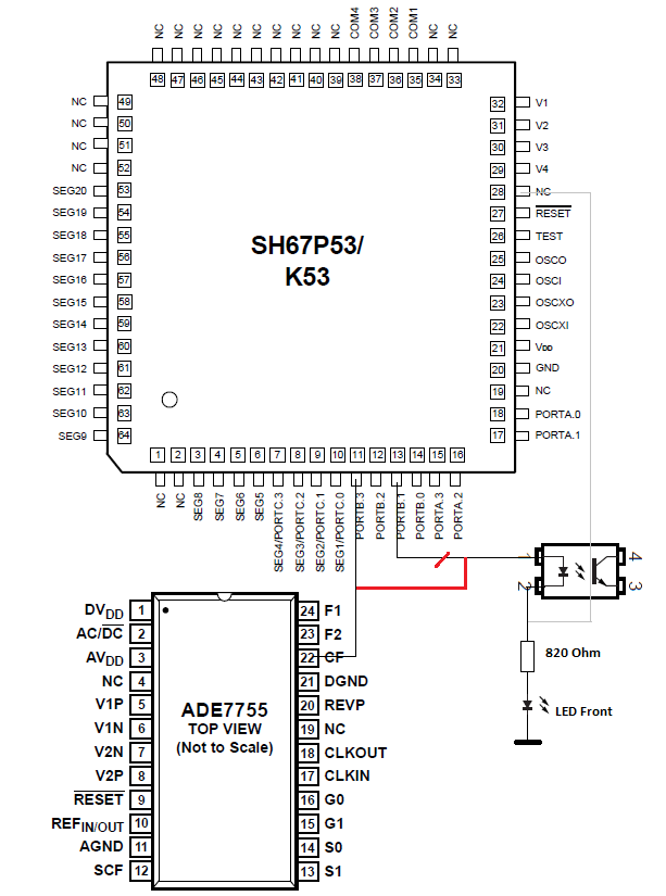
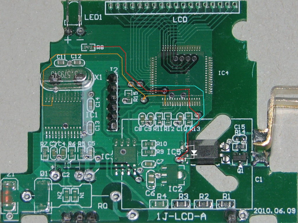
See schematic below. Black wires are already there. Grey wires are also there but only for layout purposes. The red wire shows, where u have to work.
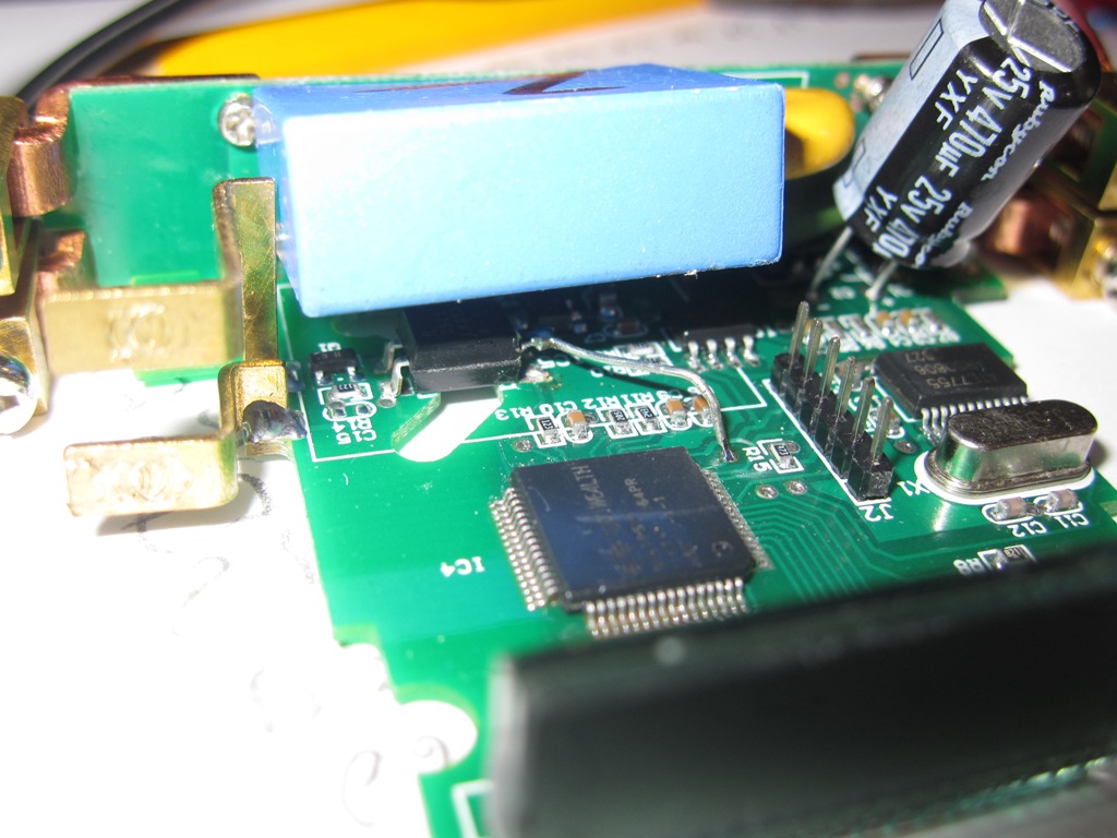
It's very easy to do. Just lift one pin of the Optocoupler and connect it to a via as shown in the picture.
And you're done!
Result
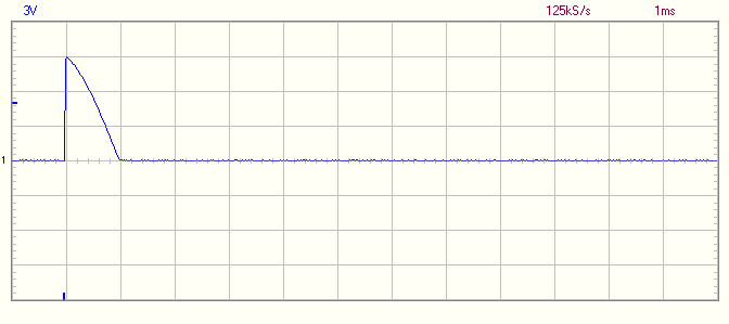
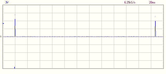
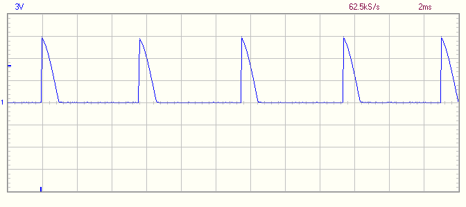
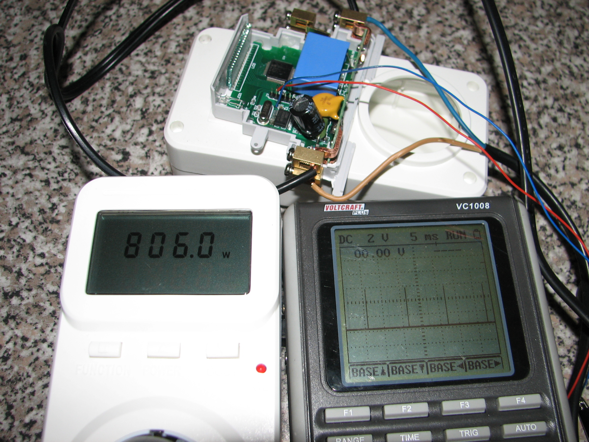
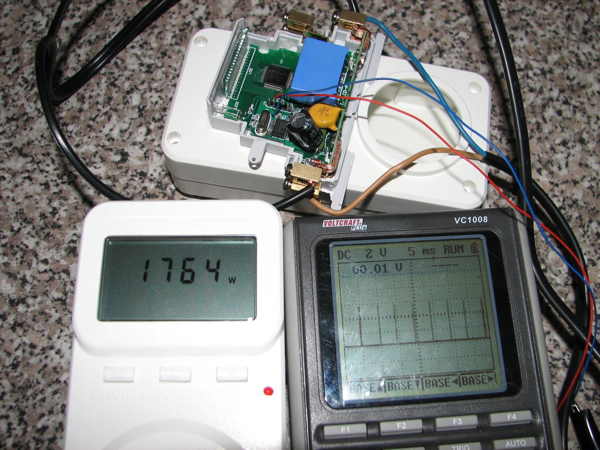
Signal output with a 2,7k pull-down and 9V battery on S0 Output.
One Peak:
40W Bulb
2000W Hair dryer
Calibration
Calibration can be done very easy when you read out the eeprom.
The value on 0x03 multiplied by 2000 is the High Speed imp/kWh.
In the case of the first Swissnox above: 0xCF * 2000 = 410.000 imp/kWh
I verified this, by counting the 7755 pulses between the pulses of the normal S0 output. They are exactly the value 0x03 of the eeprom!
Please note that those 410.000 imp/kWh are apparently not „set in stone“. I just modified one of my S-Watts according to the manual described here. Unfortunately I don't have the opportunity to read the eprom, but my measurements resulted in 246 „new pulses“ per „old pulse“, or 492.000 imp/kWh (error rate is <1%). I have 9 more devices to modify and will report my findings shortly.
Note that the length of a pulse drops from 70-90ms per impulse before to 0.5ms after the modification.
ToDo
Calibrate- Process these impulses to use them with vz (i am working on that) → Will be done by vzlogger.
Internals
Opening
The two halves of the case are held together by the (snapped on) covers at the terminals, and slighty glued at the bottom. Jam a large screwdriver in between the case and covers from the bottom (remove the rail clip first, also using a little violence), and pry them off (in some of my devices some glue got in there too, tough luck). then gently pry apart the side covers from the display side, until the glue breaks.
Energy Metering IC
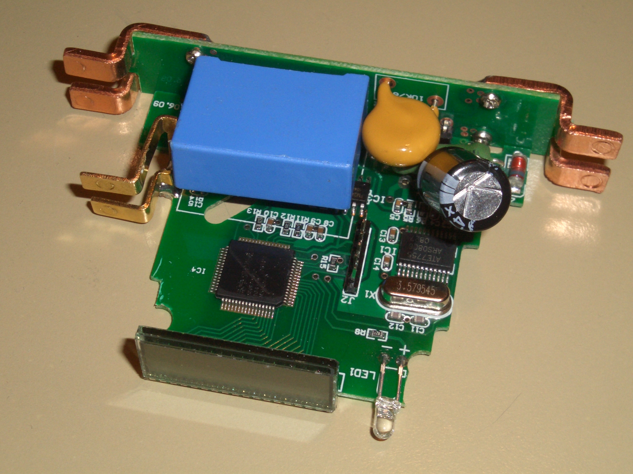
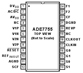
The chip is labeled „ATE7755“, but google turns up nothing for that. It appears that it's a clone of the analog devices ADE7755. All pins i checked so far match the ADE7755 pinout.
„Energy Metering IC with Pulse Output“ – http://www.analog.com/static/imported-files/data_sheets/ADE7755.pdf
Curiously, the only connection between the ATE7755 and the controller is the 7755's „CF“ pin, which is, according to the datasheet:
Calibration Frequency Logic Output. The CF logic output gives instantaneous active power information.
This output is intended to be used for calibration purposes. Also, see the SCF pin description.
The normal pulse output pins (F1 and F2) are not connected. The output signal to the optocoupler is generated by the controller.
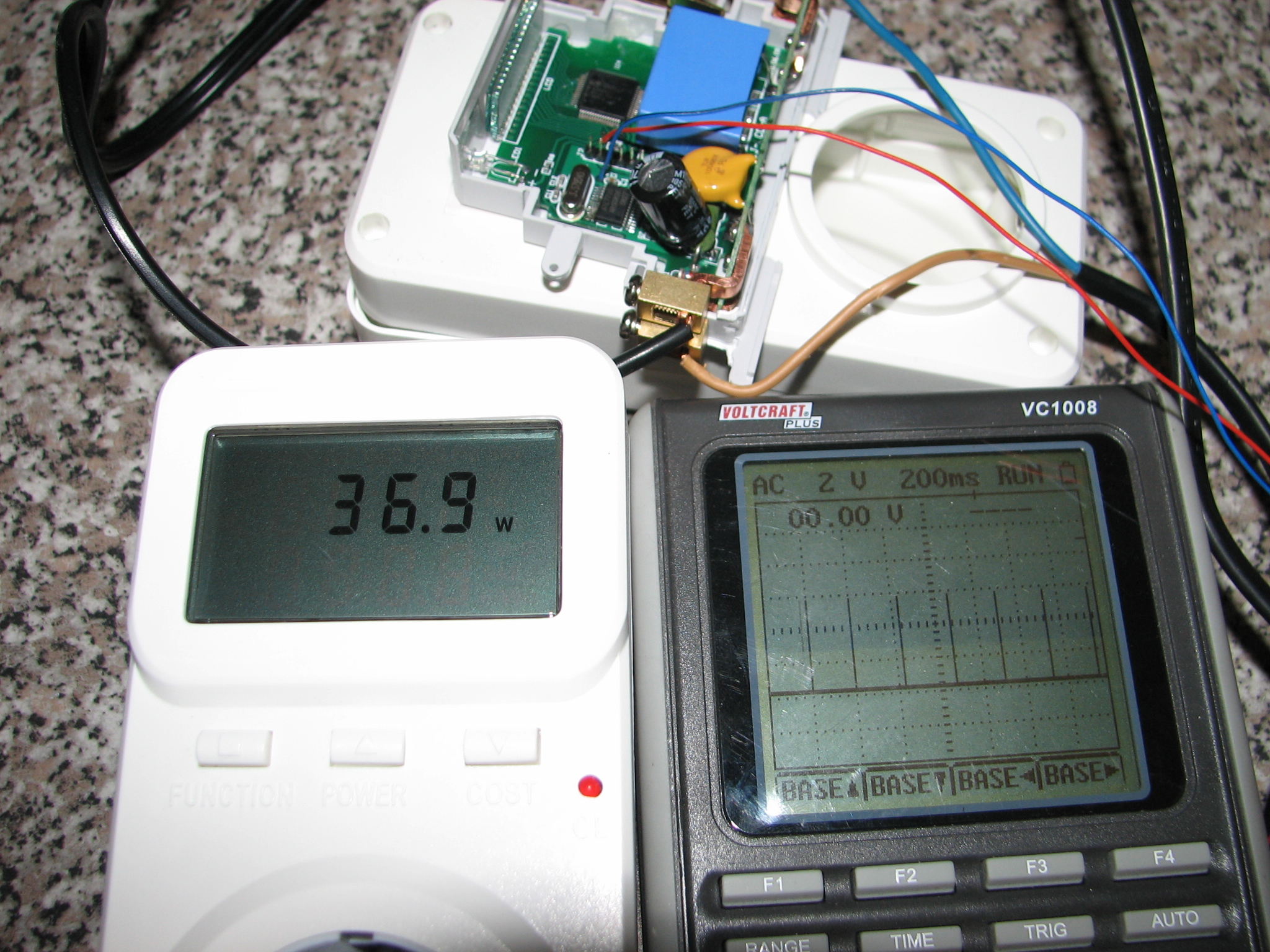
Some measurements of the signal (kd302 used as reference):
| power (approx.) | pulse distance (approx.) |
|---|---|
| 37w | 220ms |
| 800w | 11ms |
| 1760w | 5ms |
That just leaves the question of how calibration is handled.
Controller
- 4-bit OTP controller: http://www.google.com/search?q=sh67p53p
EEPROM
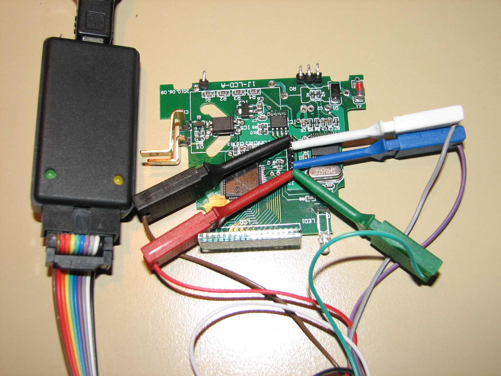
I2C>W
Power supplies ON
I2C>P
Pull-up resistors ON
I2C>[0b10100000 0 0]
I2C START BIT
WRITE: 0xA0 ACK
WRITE: 0x00 ACK
WRITE: 0x00 ACK
I2C STOP BIT
I2C>[0b10100001 r:256]
I2C START BIT
WRITE: 0xA1 ACK
READ: ...
(When the large capacitor(?) is connected, the board can't be powered from the bus pirate, because it assumes there's a short. The board in the picture has the large power supply components removed for taking pictures of the PCB.)
This is from a device that's still at 0.00kWh:
00: 0x00 0xFF 0x00 0xCF 0xFF 0xFF 0xFF 0xFF
08: 0xFF 0xFF 0xFF 0xFF 0xFF 0xFF 0xFF 0x00
[all 0xFF]
78: 0xFF 0xFF 0xFF 0xFF 0xFF 0xFF 0x10 0xFF
[all 0xFF]
E8: 0xFF 0xFF 0xFF 0xFF 0xFF 0x55 0xFF 0xFF
[all 0xFF]
F8: 0xFF 0xFF 0xFF 0xFF 0xFF 0xFF 0xFF 0x00
This is the device used for the CF measurements above, counter at 0.07kWh:
00: 0x00 0xFF 0x00 0xCD 0xFF 0xFF 0xFF 0xFF
08: 0xFF 0xFF 0xFF 0xFF 0xFF 0xFF 0xFF 0x07
[all 0xFF]
78: 0xFF 0xFF 0xFF 0xFF 0xFF 0xFF 0x10 0xFF
[all 0xFF]
E8: 0xFF 0xFF 0xFF 0xFF 0xFF 0x55 0xFF 0xFF
[all 0xFF]
F8: 0xFF 0xFF 0xFF 0xFF 0xFF 0xFF 0xFF 0x00
So the second line must be the counter value, with unused places left at 0xFF. The first line (only difference between the two) must be the calibration value?
Connectors
J2
power, calibration, programming(?)
| pin | description |
|---|---|
| 1 (at „J2“ label) | +5V |
| 2 | i2c SCL (eeprom) |
| 3 | to controller (with pull-down resistor) |
| 4 | to controller |
| 5 | i2c SDA (eeprom) |
| 6 | GND |
PCB Revisions
Either there are different versions of the device, or the above schematic is not 100% correct. Also, a not connected pin on the controller is misused to route a trace (red) under the controller. ew…
I dont think there are different versions of the device because your picture shows the same circuit as determined in the shematic above. Just the routing is different. Have a closer look.In my device, CF is connected to portA.0, your schematic connects CF to portB.3, which is i2c SCL in my device.
